1JG15-1 DC Solid State Relay
Standard
Q/RY.J0191-2005
Applications
Suitable for defense and industrial control fields, such as power distribution program, solenoid valve control, motor control, pyrotechnic control, computer interface, digital circuit interface, signal transmission, numerical control equipment and measuring instruments, suitable for harsh environments.
| Technical Parameters | Min. | Typ. | Max. | Unit | |
| Input Parameters | |||||
| Input voltage | 28 V | 18 | 28 | 32 | Vd.c. |
| 12 V | 10 | 12 | 14 | ||
| 5 V | 4 | 5 | 7 | ||
| Input bias current | 15 | mA | |||
| Input control current | 10 | mA | |||
| Switch-on Voltage | 28 V | 18 | Vd.c. | ||
| 12 V | 9 | ||||
| 5 V | 3.6 | ||||
| Shutdown voltage | 28 V | 5 | Vd.c. | ||
| 12 V | 1.5 | ||||
| 5 V | 1.5 | ||||
| Switch On time | 5000 | μ s | |||
| Switch off time | 1000 | μ s | |||
| Reverse polarity | 14/32 | Vd.c. | |||
| Output parameters | |||||
| Number of output circuit groups | 1D | ||||
| Output current | 1×10⁻⁴ | 15 | A | ||
| Output voltage | 1 | 30 | Vd.c. | ||
| Output voltage drop | 0.3 | Vd.c. | |||
| Output leakage current | 20 | μ A | |||
| Transient Voltage | 60 | Vd.c. | |||
| Overload | 70 | A | |||
| Electrical insulation parameters | |||||
| Insulation resistance | 500 | MΩ | |||
| Dielectric withstand voltage | 1000 | Vr.m.s. | |||
| Isolated capacity | 25 | pF | |||
| Environmental parameters | |||||
| Seal leak rate | 1×10⁻¹ | Pa·cm3/s | |||
| Random vibration | 40 10~2000 |
(m/s2)2/Hz, Hz | |||
| Constant acceleration | 980 | m/s2 | |||
| Shock | 980, 6 | m/s2, ms | |||
| Storage temperature | -55~125 | ℃ | |||
| Operating temperature | -55~105 | ℃ | |||
| Other parameters | |||||
| Weight | 35 | g | |||
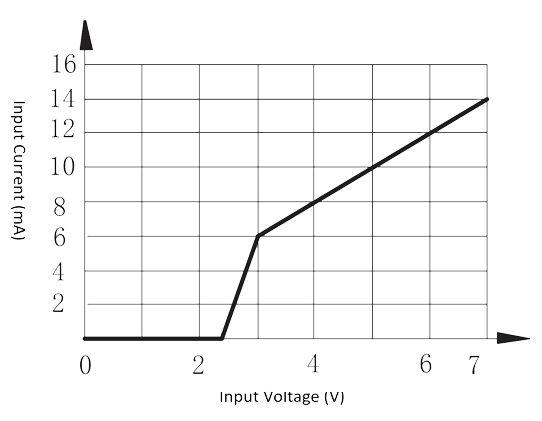
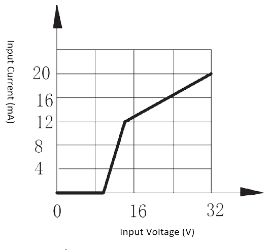
| Figure 1a. Input current vs. Input voltage (5 V) | Figure 1b. Input current vs. Input voltage (28 V) |
 |
 |
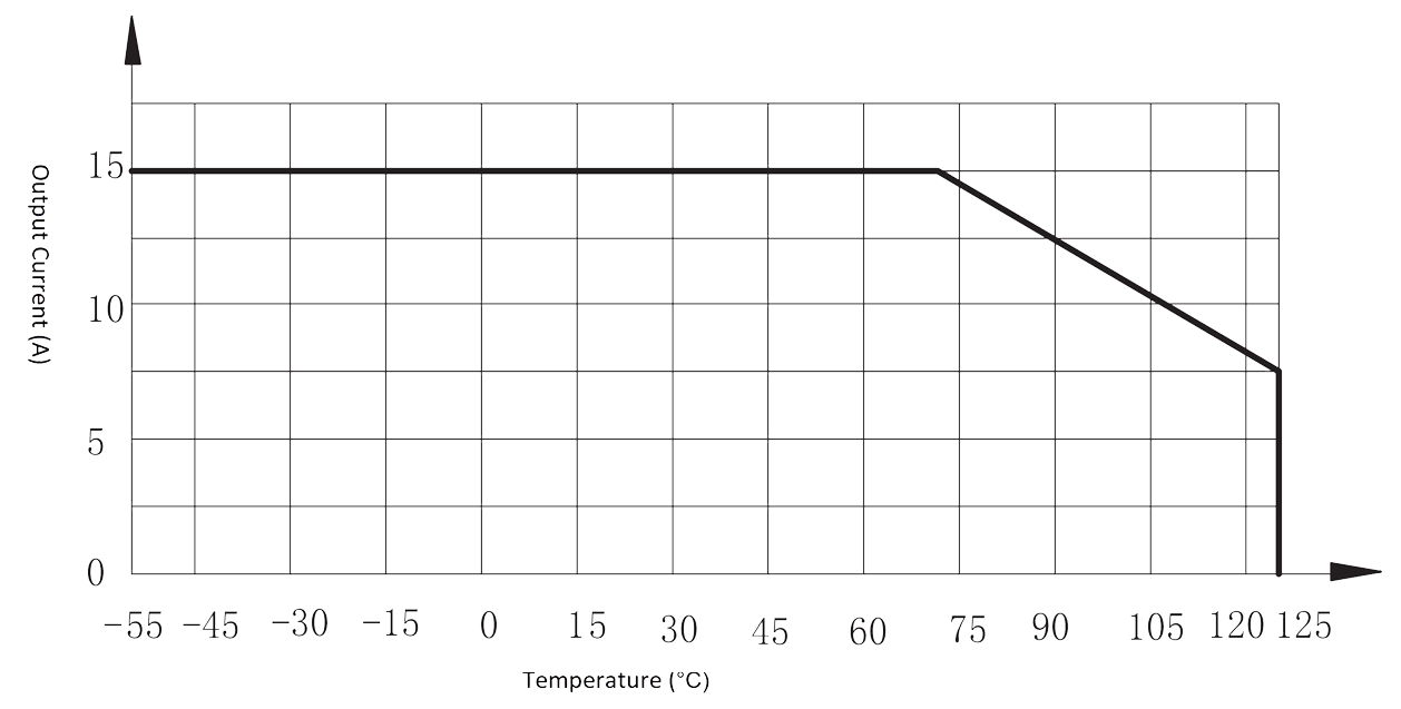
| Figure 2. Maximum output current vs. ambient temp. | |
 |
|
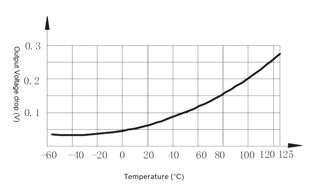
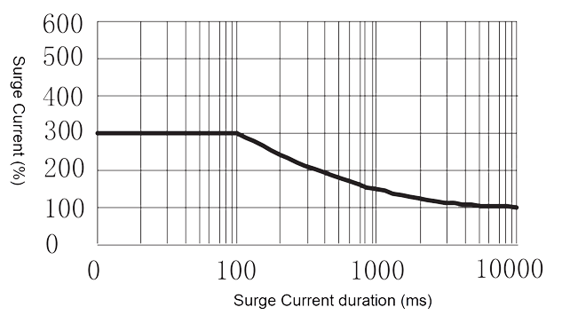
| Figure 3. Output voltage drop vs. temperature | Figure 4. Peak Surge Current vs. Surge Current Duration |
 |
 |
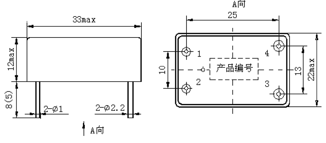
Mechanical drawings |
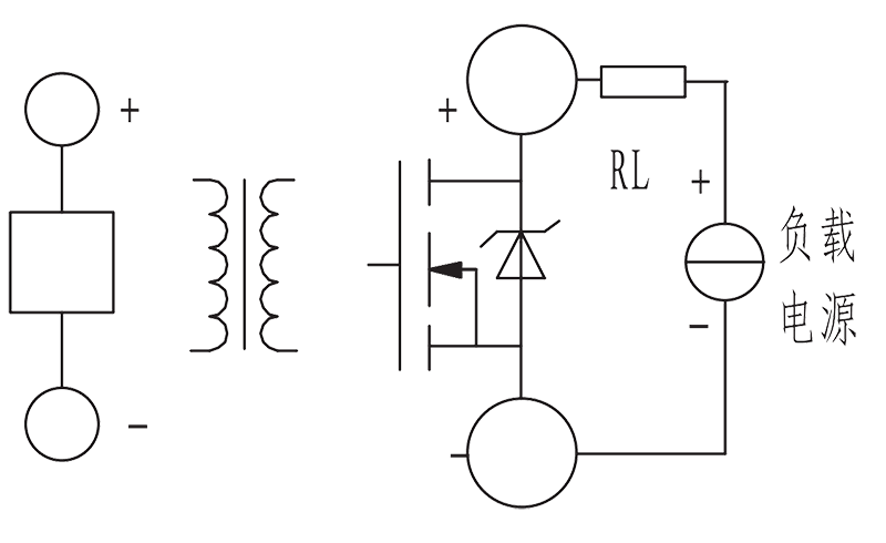
Bottom view Circuit |
 |
 |
Order Mark
Example: 1JG15–1 001Y
| 1 | JG | 15 | – | 1 | 001 | Y |
| Number of outputs | Solid relay main name | Rated output current | Design Number | Specification No. (005: 5V, 028: 28V) | Screening level (Y or W) |