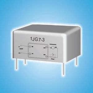
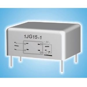
1JG2-3 DC Solid State Relay
Standard
Q/RY.J01131.2-2007
Application
Suitable for defense and industrial control fields, such as computer interfaces, digital circuit interfaces, signal transmission, numerical control equipment and measuring instruments, suitable for harsh environments.
Description
- Overload can be customized according to special requirements.
| Technical Parameters | Min. | Typ. | Max. | Unit |
| Input Parameters | ||||
| Input voltage | 3.6 | 5 | 7 | Vd.c. |
| Input current (5V) | 8 | 10 | mA | |
| Guaranteed turn-on voltage | 3 | Vd.c. | ||
| Guaranteed turn-off voltage | 1.5 | Vd.c. | ||
| Switch On time | 50 | μ s | ||
| Switch off time | 300 | μ s | ||
| Reverse polarity | 7 | Vd.c. | ||
| Output parameters | ||||
| Number of output circuit groups | 1H (1 group N.O.) | |||
| Output current | 1×10⁻³ | 2 | A | |
| Output voltage | 1 | 60 | Vd.c. | |
| Output voltage drop | 0.2 | Vd.c. | ||
| Output leakage current | 10 | μ A | ||
| Transient voltage | 70 | Vd.c. | ||
| Overload | 5 | A | ||
| Electrical insulation parameters | ||||
| Insulation resistance | 1000 | MΩ | ||
| Dielectric withstand voltage | 750 | Vr.m.s. | ||
| Isolated capacity | 25 | pF | ||
| Environmental parameters | ||||
| Seal leak rate | 1×10⁻² | Pa·cm3/s | ||
| Random vibration | 40
10~2000 |
(m/s2)2/Hz, Hz | ||
| Constant acceleration | 49000 | m/s2 | ||
| Shock | 14700, 0.5 | m/s2, ms | ||
| Storage temperature | -55~125 | ℃ | ||
| Operating temperature | -55~105 | ℃ | ||
| Other parameters | ||||
| Weight | 4 | g | ||
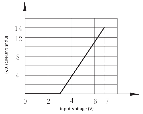
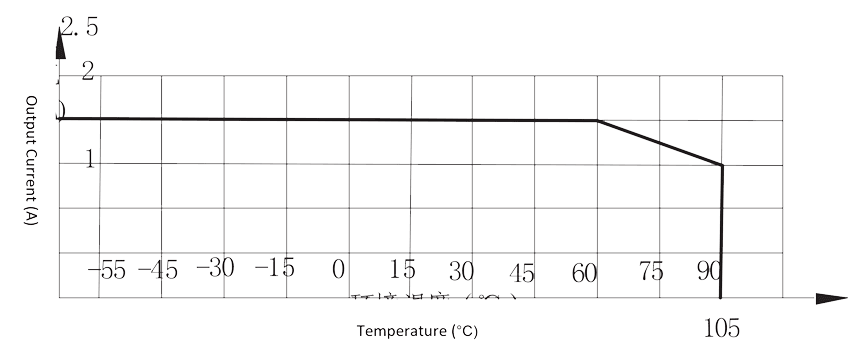
| Figure 1. Input current vs. Input voltage curve | Figure 2. Maximum output current vs. ambient temp. |
 |
 |
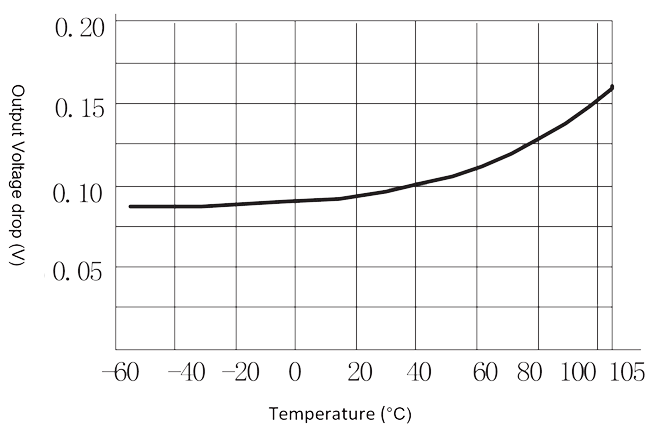
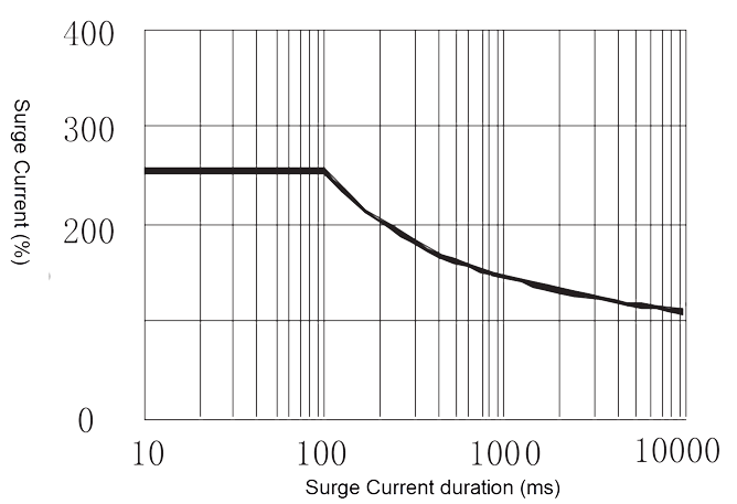
| Figure 3. output voltage drop vs. temperature curve | Figure 4. Peak Surge Current vs. Surge Current Duration |
 |
 |
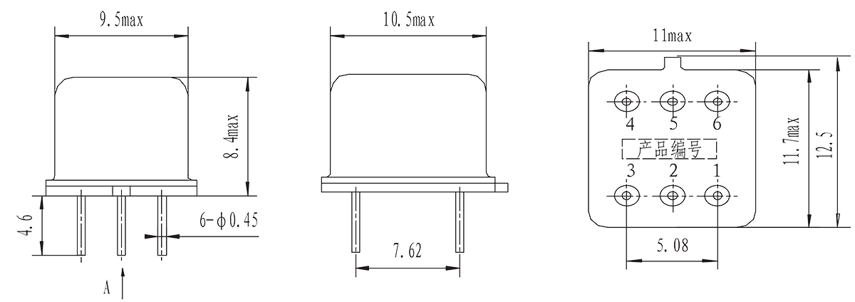
Mechanical drawings |
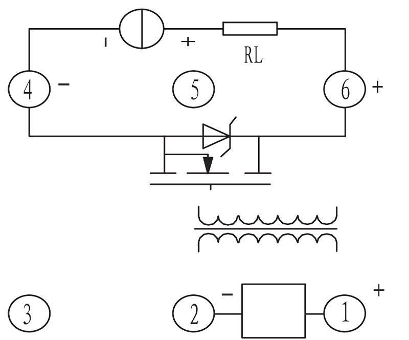
Bottom view Circuit |
 |
 |
Order Mark
Example: 1JG2-3Y
| 1 | JG | 2 | – | 3 | Y |
| Number of outputs | Solid relay main name | Rated output current | Design Number | Screening level (Y or W) |
Note: Please specify the screening level (Y or W) or special demands when ordering.